102 Minimum Theremin Assembly
Instructions
(Back to "Technical
Information")
These instructions contain steps to assemble these Harrison
Instruments
102 Minimum Theremin Kit products:
102-KIT - Complete kit with all the parts to
construct a 102 Minimum
Theremin
102-PCBKIT1 - Unpopulated
printed circuit board
(PCB) with user-soldered, on-board components
102-PCBKIT2 - Unpopulated printed circuit board
(PCB) with user-soldered
on-board and off-board components
Before you begin, verify that
all the parts have been
included in your kit. Click on the link that matches your kit's product
number:
Beginners are encouraged to learn about proper soldering
techniques before assembling this kit. Internet instructional videos on
the topic are available:
Curious
Inventor
Basic Soldering Lesson 1
-
"Solder & Flux" (PACE,
Incorporated; 8 additional lessons available)
Click here for
images of a properly soldered
kit.
Click here
for the 102 Minimum
Theremin Troubleshooting Guide.
The troubleshooting guide contains valuable advice that will
be helpful
to you in your construction.
It is recommended that you read this guide before you begin
soldering.
You will need:
1. One of the 102 Minimum
Theremin Kit products: 102-KIT,
102-PCBKIT1, or 102-PCBKIT2
2. Tools, available from distributors such as
All-Spec Industries,
Allied Electronics,
and
Mouser Electronics:
- Wire Strippers, such as Xcelite type 100X
- Diagonal Cutters, such as Xcelite type MS54J
- Long-Nose Pliers, such as Xcelite type LN54
- #1 Phillips Screwdriver, such as Xcelite type
X101
- 1/8" Flat-Blade Screwdriver, such as Xcelite
type R186
- 5/16" Nut Driver, such as Xcelite type HS10
- 3/8" Nut Driver, such as Xcelite type HS12
- 7/16" Nut Driver, such as Xcelite type HS14
- 1/2" Nut Driver, such as Xcelite type HS16
- Adjustable Wrench, such as Xcelite type 46CG
- Small-wattage Soldering Iron Station, such as
Weller type WTCPT
- Solder
Tin/Lead Alloy,
such as Kester type 24-6337-0027: 63% Tin - 37% Lead, with Rosin Core,
0.031" diameter
or
Tin/Silver/Copper Alloy,
such as Kester type 24-7068-1402: 96.5% Tin - 3% Silver - 0.5% Copper,
with Rosin Core, 0.031" diameter
|
Choosing
the Type of Solder
Either Tin/Lead
Alloy solder, or Tin/Silver/Copper
Alloy solder may be used to construct this kit.
Tin/Silver/Copper
Alloy solder was introduced in the early 2000s to comply
with an environmental
directive known as the Restriction of Hazardous Substances Directive,
"RoHS."
Click
here for more information on the RoHS directive.
All the parts in this kit are compliant with the
RoHS directive. However, the finished kit will not be
in compliance with the RoHS directive if it is constructed
with Tin/Lead Alloy
solder.
There are differences between the two
solder types:
Tin/Silver/Copper Alloy
solder requires a higher melting temperature than Tin/Lead Alloy solder,
and persistent application of excessive heat may damage the kit's
printed circuit board and
components.
The flow characteristic and adhesion of Tin/Silver/Copper
Alloy solder is inferior to that of
Tin/Lead Alloy
solder, making it more difficult to apply.
Tin/Silver/Copper
Alloy connections are duller than connections made with Tin/Lead Alloy solder
and are harder to evaluate for reliability because of their clumpy,
granular appearance.
The successful use of of Tin/Silver/Copper Alloy solder
generally requires a greater degree of
experience than the use of Tin/Lead
Alloy solder.
Tin/Lead
Alloy solder, when used responsibly, poses no health
threat to the kit builder or user,
and is generally recommended. However, the responsible use of either
type of solder includes
the following precautions:
1) Do not put solder in your mouth.
2) Do not put your hands in your mouth or rub your eyes after handling
solder.
3) Wash your hands thoroughly with soap and water after handling solder.
4) Use a temperature-controlled soldering iron that limits soldering
temperatures to 700şF (371şC).
5) Provide adequate air-flow and ventilation to remove solder flux
fumes from your workplace.
6) Wear safety glasses and suitable clothing to protect your eyes and
body from hot solder.
IMPORTANT:
Regardless of the type of solder alloy you choose, only use solder with
a
rosin core. Do not use "water soluble flux" or
"acid flux" core types.
|
Assembly Instructions
-
Mild Oxidation of the
printed circuit board (PCB) solder pads may have
occurred during storage or transit. To clean them, gently rub the pads
with an unused pencil eraser. Remove any eraser residue with a clean,
lint-free cloth.
-
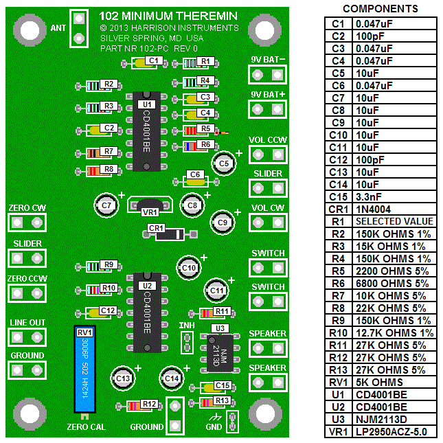
In the following steps,
you will solder the components to the PCB. This image illustrates the
completed PCB, and may be used as a reference.
In the illustration, the COMPONENTS table uses abbreviations: "uF"
means microfarads, "pF" means picofarads, "nF" means nanofarads, and
"K" means 1000. As examples, "0.047uF" is verbalized as "Zero point
zero four seven microfarads, and "150K OHMS" is verbalized as
"One-hundred-fifty-thousand ohms."
-
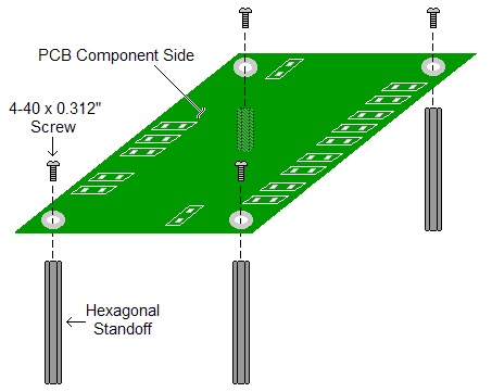
Attach a hexagonal
standoff to each corner of the PCB with a 4-40 x
0.312"L screw, as illustrated. The screws are inserted into
the PCB's component side, which is the side with the white printing.
The hexagonal standoffs extend from the PCB's bottom side. The
hexagonal standoffs elevate the board from the work surface to allow
the easy insertion of components.
-
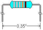
Form the leads of Resistor
R1 with long-nose pliers, as shown. (Note
that R1 has a SELECTED VALUE.
Its ohm-value is selected at the factory to best-match the
characteristics for the circuit. Therefore, R1's first three color
bands will vary from kit to kit, and these three bands are shown here
as white only for the purpose of illustration.)
- Insert resistor
R1 into the PCB at the location marked "R1." Note that the resistors in
this kit may be oriented in either direction. However, it is good
practice to orient them so that the color bands representing their
values are read from left to right. Click
here for a Resistor
Identification Guide.
- Cut off the resistor's excess lead lengths,
leaving about 1/16th inch of each lead extending from the board's
bottom, as shown in "METHOD 1," below. If you desire, you may bend the
resistor's leads against the board's pads, as shown in "METHOD 2," and
then cut them. Doing so will help keep the resistor in place when the
board is turned over for soldering. The same choice of these two
methods applies to all the other components. The disadvantage of METHOD
2 is that a component will be harder to remove in the event that it has
to be replaced. If you choose METHOD 2, make sure that the bent-over
leads do not touch each other or adjacent leads or solder pads. Save
two of the cut-off resistor leads to make a jumper for step 20 and
optional step 24.

- Solder resistor R1 in
place. If you used "METHOD 1," above, you can solder one or both of the
leads on the top side of the board to keep it in place. Then, turn the
board over to solder both leads on the bottom side. Top-soldering the
leads is optional, but useful for keeping the resistor from falling out
of the board when METHOD 1 is used. For either method, it is standard
practice to always solder the leads on the bottom of the board.
Note: If desired, flux residue from solder may optionally be removed
from the PCB with 90% Isopropyl Alcohol, applied with the gentle
scrubbing action of a toothbrush. Absorb the used alcohol with a paper
towel, and repeat as required until all the flux is removed. Flux
removal will be easier if done shortly after connections are soldered.
Confine scrubbing only to the solder pad areas, as directly scrubbing
components may remove their markings or otherwise damage them. Flux may
also be removed from other soldered connections, such as the terminals
on controls and jacks, with a brush and alcohol. However, be sure to
keep the alcohol confined to the part being cleaned by using adequate
absorbent paper towel as a "dam" to prevent it from spreading
to
adjacent surfaces. WARNINGS:
Isopropyl Alcohol is highly flammable, and should be kept away from
heat sources such as soldering irons. Use Isopropyl Alcohol in a
well-ventilated area. Do not use the toothbrush for personal hygiene
after it is used for PCB cleaning.
- Repeat steps 5 through 8 for the remaining 12
resistors, using the illustration in step 2 as a guide.
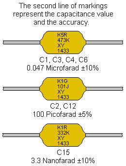
- Prepare the leads of capacitors C1,
C2, C3, C4, C6, C12, and C15 the same way
the resistors were prepared, and solder them in their respective
locations on the PCB. These capacitors may be oriented in either
direction, however, it is good practice to orient them so that their
second line of numerical markings face upward, read from left-to-right.
The second line of markings are three digits followed by a letter, and
designate the capacitor value and accuracy. (The first line represents
the manufacturer, voltage, and the kind of material used to make the
capacitor. The third line is a lot code, and will vary, as will the
fourth line, which is a coded date of manufacture.) IMPORTANT: These
capacitors are very delicate. Do not apply excessive force to their
leads. Make sure the capacitors fit easily into the PCB before
soldering, because any tension on the leads will cause them to break
off the capacitor body while being soldered.
- In the next steps, rectifier
CR1 and four integrated circuits (U1,
U2, U3, and VR1) will be installed into
the PCB. IMPORTANT:
These are semiconductor devices that are sensitive to static electricity.
Static electricity
is a charge that accumulates on your body's surface and on other
objects. You can often observe static electricity's effect when you
touch a doorknob or other metal object and feel a brief jolt in your
hand. While usually harmless to people, it can destroy semiconductors
such as those used in this kit. To prevent damage to these
semiconductors, discharge static electricity from your body by touching
a grounded metal object near your workstation before removing the
semiconductors from their conductive foam pad or conductive bag. Unwrap
the semiconductors at your workstation, and install them in the PCB
immediately. Click Here for Component
Handling Precautions.
- The CR1 rectifier that comes with your kit may
have adhesive tabs attached to their leads. If so, cut them off as
shown:

Form the leads of rectifier CR1 as
shown:
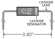
- Insert rectifier CR1 into the PCB at the
locations marked "CR1." IMPORTANT:
Rectifier CR1 must be inserted in the correct direction.
Make sure that its CATHODE LEAD is inserted into the PCB hole with the
SQUARE PAD, closest to the right edge of the PCB. As shown in the picture, the cathode lead is
the lead designated by the CATHODE DESIGNATOR band on the rectifier's
body. Cut off the rectifier's excess lead lengths, leaving about 1/16th
inch of each lead extending from the board's bottom. Once CR1 is
correctly inserted, solder it in place.
- Refer to the following picture of integrated
circuits U1 and U2.
Note the notch that designates the end of the device with pins 1 and
14. The ICs may be supplied with their pin rows angled slightly apart.
To facilitate their insertion into the PCB, gently
form the pin rows so that they are 90 degrees (perpendicular) with
relation to the body of the IC. This may be done by carefully pressing
each row against a flat surface (such as a tabletop) just enough to
bend them perpendicular with the body.
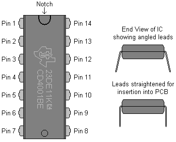
- Insert ICs U1 and U2
into the PCB at the locations marked "U1 and U2." IMPORTANT: U1 and
U2 must be inserted in the correct direction. Make sure that pin 1 is
inserted into the upper-left PCB hole with the SQUARE PAD. As shown in the picture, the end of the IC
with pin 1 is designated by the U-shaped notch on the IC's body. Do not confuse the U-shaped notch
with the circular recess that may be present at the other end of the
IC's package. Before
soldering the ICs into place, verify that they are oriented correctly
and that none of the pins have been bent, which would prevent them from
going through their holes. Once the ICs are correctly inserted, solder
them in place. Solder two of each of the IC's pins on the
top side of the board to keep them in place; for example, pins 7 and
14. Then, turn the board over to solder all the pins on the bottom side.
IMPORTANT: Avoid excessive heat when soldering U1 and U2.
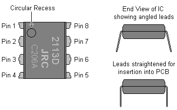
- Refer to the following picture of integrated
circuit U3. As with the previous two
ICs, gently form U3's pin rows so that they are perpendicular with
relation to the body of the IC. Insert IC U3 into the PCB at the
location marked "U3." IMPORTANT:
U3 must be inserted in the correct direction. Make sure
that pin 1 is inserted into the upper-left PCB hole with the
SQUARE PAD. As
shown in the picture, the end of the IC with pin 1 is designated by the
circular recess on the IC's body. Before soldering U3 into
place, verify that it is oriented correctly and that none of its pins
have been bent, which would prevent them from going through their
holes. Once U3 is correctly inserted, solder it in place. Solder
two of U3's pins on the top side of the board to keep it place; for
example, pins 4 and 8. Then, turn the board over to solder all the pins
on the bottom side. IMPORTANT: Avoid excessive
heat when soldering U3.
- Form the leads of integrated circuit
VR1 with long-nose pliers as shown. IMPORTANT:
The regulator leads are brittle and will break easily.
Form the leads gently, avoiding excessive plier pressure and sharp
bends.
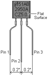
- Insert VR1 into the PCB at the location marked
"VR1." IMPORTANT:
VR1 must be inserted in the correct direction. Make sure that pin 1 is
inserted into the PCB hole with the SQUARE PAD closest to the left edge
of the PCB. As
shown in the picture, pin 1 is the pin on the left when VR1 is oriented
with the flat surface facing you and the pins are pointing downward.
Cut off VR1's excess lead lengths, leaving about 1/16th inch of lead
extending from the board's bottom. Once VR1 is correctly inserted,
solder it in place. IMPORTANT: Avoid excessive
heat when soldering VR1.
- Insert pitch zero trimmer
potentiometer RV1 into the PCB at the location marked "RV1."
The adjusting screw of the potentiometer is closest to the bottom edge
of the board. Once RV1 is correctly inserted, solder it in place,
making sure that it is held flat against the board.
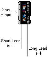
- Insert Capacitors C5, C7, C8, C9,
C10, C11, C13 and C14 into the PCB at their respective
locations. Refer to the illustration below to identify their positive
(+) leads. IMPORTANT:
These eight capacitors must be inserted in the correct
direction. Make sure that their longer (+) leads are inserted into the
PCB holes with the SQUARE PADS closest to the right edge of the PCB.
Cut off the
capacitors' excess lead lengths, leaving about 1/16th inch of each lead
extending from the board's bottom. Solder them in place.
- Refer to the illustration below to form a
piece of resistor lead saved from step 6 into a "U" shaped jumper, and
insert it between the two pads marked GND in the
lower-right of the PCB. Cut off the excess lead lengths, leaving about
1/16th inch of each lead extending from the board's bottom. Solder the
jumper in place.
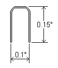
A second jumper may be soldered between the two pads marked "INH," located to the
left of U3.
This will disable the SPEAKER
output for your theremin by shutting-down the U3 amplifier IC, and
reduce battery drain. If you do not plan to connect a loudspeaker
directly to the PCB's SPEAKER
pads, and only require an output from LINE OUT, you may
insert this jumper. Do not insert this jumper if the
PCB will be used to directly drive a loudspeaker.
- All of the components have now been attached
to the PCB. Inspect each soldered connection carefully to ensure that
there are no solder bridges between adjacent pads, pads with excess
solder, or insufficient solder. Ensure that the three ICs,
voltage regulator, rectifier, and capacitors C5, C7, C8, C9, C10, C11,
C13 and C14 are inserted in the correct direction.
For product number
102PCB-KIT1, you have completed your kit.
For product number 102PCB-KIT2, the following steps will provide
instructions for adding the peripheral parts to your circuit board.
For product number 102-KIT, skip steps 22 through 25, and proceed with step 26.
IMPORTANT:
Do not perform steps 22 through 25 for product
number 101-KIT.
|
- With the exception of the antenna wire, the
lengths of the wires connecting the PCB to the off-board components are
not critical, and should be selected for your choice of enclosure and
control locations. Plan in advance by making the wires long enough to
allow the circuit board be to mounted as desired, with the peripheral
parts mounted through the enclosure's side or sides. Note that 102PCB-KIT2 is
provided with 4 feet of hookup wire, which should be an ample amount
for any reasonable arrangement.
Pay careful attention to the connection order for all the wires. The wire pairs going to the power
switch and speaker, however, may be
connected in either order.
The PCB should be mounted in a position that
permits the adjustment of the pitch zero trimmer potentiometer ("ZERO
CAL" trimmer).
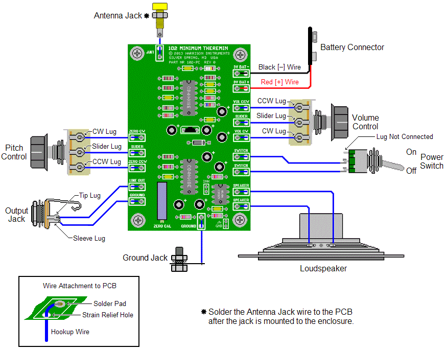
Refer to the illustration below. Using hookup wire,
connect the pitch control, output jack, ground jack,
loudspeaker, power switch, and volume control to
the PCB. The battery connector is furnished with red (+) and black (-) wires that
are also soldered to the PCB. Note the detail in the lower-left of the
drawing illustrating how the wires are attached to the PCB. Passing the
insulated part the wires through the strain relief holes will prevent
them from breaking off the solder pads. Note that the
output jack has two solder lugs, one
called the "tip lug," and the other the "sleeve lug." These
must not be interchanged. The lugs can be identified by their
different shapes:  is
the tip
and
  is the
sleeve. The sleeve lug may
also be identified as the one with "SWITCHCRAFT" stamped into the metal
where it extends from the jack. The tip lug is connected to the "LINE
OUT" pad on the PCB, and the sleeve lug is connected to the "GROUND"
pad on the PCB.
You may connect wire to the antenna jack now, but
don't solder the other end of its wire to the PCB until it is mounted
through the wall of your enclosure, since this jack cannot pass through
the enclosure wall from the rear.
The antenna wire length should be just enough to go between the antenna
jack and the PCB, plus a little slack. If you are providing your own
metal enclosure, be sure that the wire between the antenna jack and the
PCB isn't pressed against a metal surface. Excessive antenna wire
length, or locating the antenna wire too close to metal parts has the
effect of increasing the amount of capacitance presented to the
theremin circuit's antenna input. Excessive capacitance will prevent
the theremin from functioning.
- Attach knobs
to the pitch control and
volume control with the allen
keys provided. The knobs have a white index line which
indicate the control's degree of rotation. You may position the index
line so that it is approximately in the 7 o'clock position when the
control shaft is fully counterclockwise, and approximately in the 5
o'clock position when the shaft is fully clockwise. Once the controls
are mounted to an enclosure, the knobs may be repositioned as needed. Power will be "ON"
when the switch toggle in the "UP" position, as illustrated. The top
switch lug is not connected. The power switch wires may be interchanged
without affecting operation.
- Some builders may use the theremin only to
drive an external amplifier/speaker system, and not require the speaker
furnished with the kit. In this case, battery life may be improved
considerably by inserting a jumper formed from a piece of resistor lead
saved from step 6 between the two pads marked "INH"
located to the left of U3. Cut off the excess lead
lengths, leaving about 1/16th inch of each lead extending from the
board's bottom. Solder the jumper in place. Do not insert
this jumper for the normal operation of the theremin with the supplied
speaker.
| For
product number 102PCB-KIT2, you have completed your kit.
|
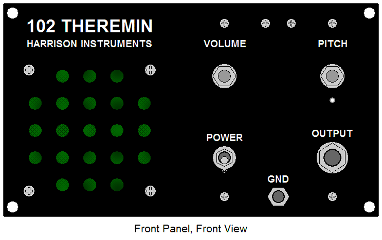
- The following steps provide instructions to
attach parts, including the PCB, to the front panel,
and to wire them together.
- Use
these illustrations as a reference in
attaching parts to the front panel.
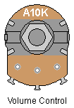
- In
the next two steps, you will attach the controls to the panel. Your kit
comes with two different controls. They have very similar appearances,
but different ohm values. They must not be interchanged. Identify
the VOLUME control, which has "A10K"
printed directly above its threaded bushing, as shown
below.

Remove
the nut and two washers from the VOLUME
control's bushing.
Referring to the "Front Panel, Rear View" illustration in step 26,
insert the VOLUME control into the appropriate panel hole through the
rear of the panel, aligning the control's anti-rotation tab with the
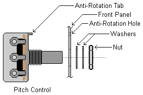
anti-rotation hole. Referring to the illustration below, fasten the
control in place with the nut and washers. Place both washers on the
threaded bushing, followed by the nut. Tighten the nut with a 7/16" nut
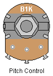
driver.

- Identify the PITCH control,
which has "B1K" printed directly above its
threaded bushing, as shown below.

Remove
the nut and two washers from the PITCH
control's
bushing. Referring
to the "Front Panel, Rear View" illustration in step 26, insert the PITCH
control into the appropriate panel hole through the rear of the panel,
aligning the control's anti-rotation tab with the anti-rotation hole.
Referring to the illustration below, fasten the control in place with
the nut and washers. Place both washers on the threaded bushing,
followed by the nut. Tighten the nut with a 7/16" nut driver.
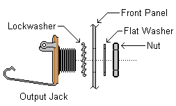
- The
OUTPUT jack is
supplied with a nut, flat washer, and internal-tooth lockwasher.
Referring to the illustration below, place
the lockwasher on the jack's bushing, then insert the jack into the
appropriate panel hole through the rear of the panel. Place
the flat washer on the jack's bushing, followed by the nut. Position
the jack
so its solder lugs are closest to the vertical edge of the panel.
Tighten the nut with a 1/2" nut driver. Tighten
the nut firmly. The teeth of the lockwasher must
pierce the non-conductive finish on the front panel so that the jack
makes good electrical contact to the panel.

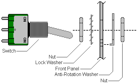
- The POWER switch is
supplied with two nuts, a lockwasher, and an anti-rotation washer. The
anti-rotation washer is illustrated below.
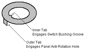
Referring to the illustration below, place one of the two nuts on the
switch bushing, and finger-tighten the nut until it is flush with the
switch body. Then, place the lockwasher on the bushing. Insert
the POWER switch into
the appropriate panel hole through the rear of the panel. Next, place
the anti-rotation washer on the bushing, engaging the washer's inner
tab in the switch's bushing groove and the washer's outer tab in the
panel's anti-rotation hole. Then, place the second nut on the bushing.
Make sure that the switch and anti-rotation washer are correctly
aligned with the panel's anti-rotation hole, and tighten the second nut
with a 1/4" nut driver.

- Wires will now be soldered to the panel
components. To assist in this step, you may temporarily remove the four
hexagonal standoffs and screws from the PCB, and temporarily attach
them to the front of the panel to keep the assembly level on your work
surface.
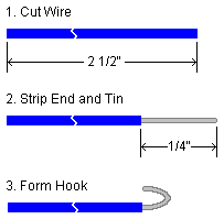
Prepare eleven 2 1/2" lengths of hookup wire as
illustrated below. Strip 1/4" of insulation from
one end of each wire. Make sure that the individual strands of the wire
remain twisted together. Pre-coat ("tin") the stripped ends with a
small amount of solder. Form each stripped end into a hook. Solder
three wires to the VOLUME control, three
wires to the PITCH control, two wires to the OUTPUT jack, and two wires
to the POWER switch. Insert the wire hooks through the holes in the
lugs, and gently squeeze them closed with pliers, so that the
wires remain in place during soldering. Only two
wires are soldered to the POWER switch. Do not solder a wire to the
switch lug located closest to the VOLUME control. The
remaining 2 1/2" wire will be used in step 33.
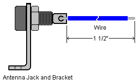
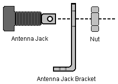
- Referring to the illustration below, attach
the antenna jack to the antenna jack
bracket with a 5/16" nut driver. Make sure the nut is
sufficiently tight, but do not strip the plastic threads.
- Referring to the illustration below, solder
the wire prepared in step 31 to the antenna jack lug. Trim the length
of the wire to 1 1/2". Strip 1/8" of insulation from the wire. Make
sure that the individual strands of the wire remain twisted together.
Pre-coat ("tin") the stripped ends with a small amount of solder.

- Attach the antenna jack bracket to the rear of
the panel as illustrated in step 26, using two #4-40
x 0.312" pan-head screws.
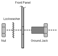
- The GND (ground) jack is
supplied with a nut, solder lug, and internal-tooth lockwasher. The
solder lug will not be used. Insert the GND jack
into the appropriate panel hole through the front of the panel.
Referring to the illustration below, place the lockwasher on the jack's
threaded bushing, followed by the nut. Tighten the nut with a 3/8" nut
driver. Tighten the nut firmly while holding the jack's front with an
open-ended or adjustable wrench. The teeth of the lockwasher must
pierce the non-conductive finish on the front panel so that the jack
makes good electrical contact to the panel.
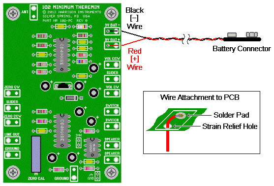
- Twist the battery connector's
wires together, and trim them to a length of 4". Strip 1/8" of
insulation from each of the wires. Referring to the illustration below,
solder the battery connector to the PCB assembly that was completed in
step 21. The battery
connector is furnished with red (+) and black (-) wires. IMPORTANT: Be careful not to
interchange the battery connector wires. Note the illustration detail showing how the
wires are attached to the PCB. Passing the insulated part the battery
connector wires through the strain relief holes will prevent them from
breaking off their solder pads.
- Remove the four hexagonal standoffs and screws
that were temporarily attached to the panel in step 31. Refasten them
to the PCB as illustrated in step 3. Set the PCB assembly aside.
- Prepare two 3 1/2" lengths of hookup
wire as illustrated below. Strip 1/4" of insulation from one
end of each wire. Make sure that the individual strands of the wire
remain twisted together. Pre-coat ("tin") the stripped ends with a
small amount of solder. Form the stripped ends into a hook.

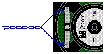
- Referring to the illustration below, solder
one wire to each of the two speaker terminals.
Insert the wire hooks through the holes in the lugs, and gently squeeze
them closed with pliers, so that the wires remain in place during
soldering. Lay the wires in the direction illustrated, and twist them
together.
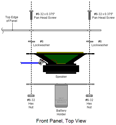
- Referring to the illustration below, attach
the speaker and battery holder to
the panel with four #6-32 x 0.375" pan head screws,
four #6 lockwashers, and four #6-32 hex
nuts. As shown, the two top screws fasten both the speaker
and the battery holder. The two sets of bottom screws, washers, and
nuts are hidden from view.

- Attach the PCB's standoffs to the panel using
four #4-40 x 0.312"
pan-head screws. Position the PCB as indicated in the illustration
below.
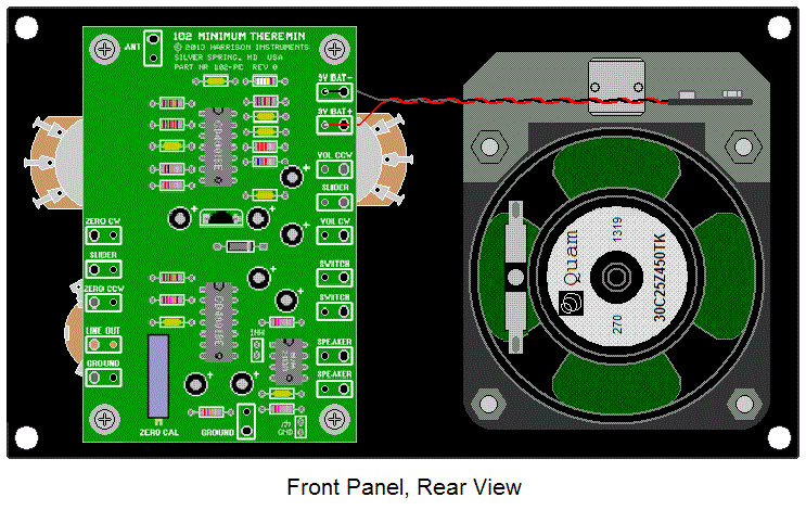
- The free ends of the panel component wires
will now be soldered into holes on the PCB. The holes are outlined with
labeled white rectangles. (Note that the hole labeled "GROUND" is not
used.) Only the smaller hole within each rectangle will be used to
solder the wire. The larger stress-relief holes will not be used. Each
wire will enter the hole from the bottom of the PCB and solder will be
applied to the top of the PCB.
Start with the speaker wires. Strip 1/8" of insulation from one end of
each wire. Make sure that the individual strands of the wire remain
twisted together. Pre-coat ("tin") the stripped ends with a small
amount of solder. Insert each speaker wire into one of the solder pad
holes on the PCB labeled SPEAKER. Solder the wires
in place.
- Repeat the above procedure for the switch
wires. Insert each switch wire into one of the solder pad holes on the
PCB labeled SWITCH. Solder the wires in place.
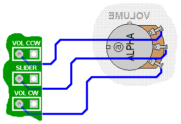
- Strip 1/8" of insulation from one end of each
wire from the VOLUME control and tin them. Solder the VOLUME control
wires to the solder pad holes on the PCB labeled VOL CCW,
SLIDER, and VOL CW. These wires must be
connected in the order illustrated below. Solder
the wires in place.

- Strip 1/8" of insulation from one end of each
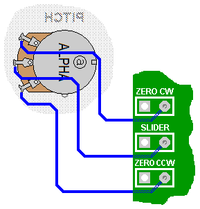
wire from the PITCH control and tin them. Insert the PITCH control
wires to the solder pad holes on the PCB labeled ZERO CCW,
SLIDER, and ZERO CW. These wires must be
connected in the order illustrated below. Solder the wires in place.

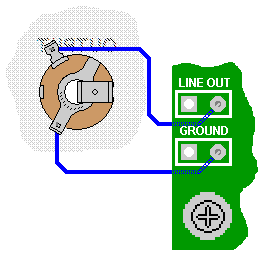
- Strip 1/8" of insulation from one end of each
wire from the OUTPUT jack and tin them. Insert the OUTPUT jack wires
into the solder pad holes on the PCB labeled LINE OUT and
GROUND. These wires must be connected in the order
illustrated below. Solder the wires in place.

- Insert the antenna jack wire into the solder
pad hole on the PCB labeled ANT. Solder the wire in
place.
- Attach knobs
to the pitch control and volume
control with the allen keys
provided. The knobs have a white index line which indicate the
control's degree of rotation. Position the index line so that it is
approximately in the 7 o'clock position when the control shaft is fully
counterclockwise, and approximately in the 5 o'clock position when the
shaft is fully clockwise.
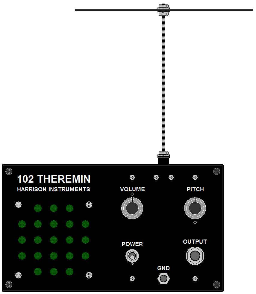
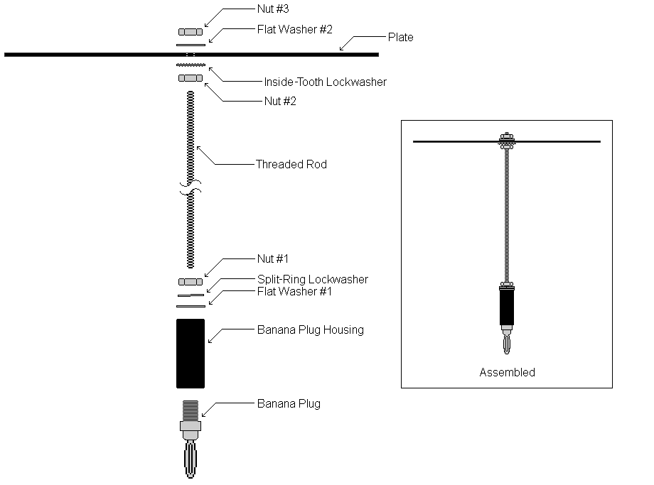
- Assemble the antenna using
the illustration below as a guide.
a. Screw the banana plug onto one end of the threaded
rod. Do not use any tools to tighten the plug; it only has to
be finger-tight.
b. Slide the banana plug housing onto the rod with
its internal-threaded end downward, and screw it onto the banana plug.
The housing also only has to be finger-tight.
c. Slide flat washer #1 onto the rod.
d. Slide the split-ring lockwasher onto
the rod.
e. Thread nut #1 onto the rod, and advance it all
the way down to the lockwasher. Hold the banana plug housing firmly and
tighten the nut with an adjustable wrench.
f. Thread nut #2 onto the rod, advancing it about
1/4" from the top.
g. Slide the inside-tooth
lockwasher onto the rod.
h. Slide the plate onto the rod.
i. Slide flat washer #2 onto the rod.
j. Thread nut #3 onto the rod.
k. Hold nut #2 with an adjustable wrench, and tighten nut #3 with a
5/16" nut driver.
Set the antenna assembly aside.
| Proceed
to the Calibration Instructions that follow. |
Calibration
Instructions
A basic understanding of the one of the theremin's operating
principles,
described in the box below, will be helpful when performing
the
calibration.
|
Theremin
Coupling
For a theremin to operate properly, sufficient
electrical coupling must exist between the player and the instrument. A
player is coupled to earth's ground
due to the relatively large
capacitance between the body and earth (about 100 to 200 picofarads).
When the theremin is connected to an external amplifier,
it is also
coupled to earth's ground via the audio output connection between the
theremin and the amplifier, which in turn, is connected to earth's
ground
by its power cord. The player's earth coupling, along with the
amplifier's connection to ground, provide the desired common connection
between the
player's body and the instrument.
When used only with its
internal loudspeaker, and not connected to an external amplifier, there
may not be sufficient electrical coupling between the
theremin and
player. This may be easily remedied by connecting the circuit's GROUND
jack to earth or a nearby metal object. If this is not practical,
attaching a wire to the GROUND jack and placing the wire in
near-proximity to the player will provide sufficient coupling. An even
simpler solution is
to simply grasp the metallic part of the theremin's
case with one hand, while playing it with the other. |
The calibration procedure will ensure that the theremin
responds correctly
to hand positions. The procedure is performed with the case removed.
After
the calibration is complete, the case will be attached, and the
theremin
will be ready for use.
- Set the POWER switch to
the down (off) position.
- Set the VOLUME control
and the PITCH control to their middle (12 o'clock)
positions.
- Attach the 9V battery to
the battery connector, and secure the battery in the holder.
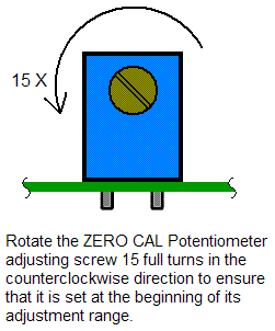
- Using a small flat-blade screwdriver, set the ZERO
CAL potentiometer on the PCB to its extreme counterclockwise
position by turning the slotted adjustment screw 15 full
counterclockwise rotations. This ensures that it is set at the
beginning of its adjustment range. Note that the potentiometer's
mechanism has an internal slip clutch, so it can safely be turned an
unlimited number of times in either direction.
- Insert the Antenna into
the antenna jack.
- Set the POWER switch to
the up (on) position.
- With one hand, hold the theremin assembly
securely by the top and bottom edges of the front panel, in an elevated
position. Hold the theremin so that you are facing the ZERO
potentiometer, and so that the antenna plate is positioned away from
you. Keep the antenna at least 4 feet away from nearby objects.
Positioning the theremin in this way enables access screwdriver access
to the ZERO potentiometer.
- With your other hand, using the small
screwdriver, slowly turn the ZERO CAL potentiometer
clockwise.
- As the ZERO CAL potentiometer
is rotated, a very high pitch will become evident. The pitch will
become successively lower with continued rotation, until it stops
abruptly. Stop turning the potentiometer at this point.
- Remove the screwdriver from the potentiometer.
Note that the pitch might return; this is a normal condition resulting
from the capacitance change that occurs when the screwdriver is removed.
- Adjust the PITCH control
just to the point where the pitch stops. This point may occur either
slightly clockwise or counterclockwise of its center position.
- Starting from a distance of about two feet,
move your hand toward the antenna. Note that the pitch commences at its
lowest frequency with your hand about 18 inches away, increasing as the
distance shortens.
- The ZERO CAL potentiometer
may be readjusted a few degrees in either direction, as
required, until the "zero beat" condition coincides with a
hand distance of 18 inches when the PITCH control
is exactly in the 12 o'clock position.
Turn the power switch off and remove the antenna.
Place the theremin into the case with
the antenna jack adjacent
to the hole in the case's top.
Secure the panel to the case with a #4-40 x 0.375" flat-head
screw
in each corner.
Insert the antenna.

Your Harrison instruments Model 102
Theremin is complete!
If you have any problems with your theremin, please e-mail us at sales@harrisoninstruments.com,
and we will be happy to resolve any difficulties. |
(Top)
Text, images, and format ©2013, 2015, 2016 by
Harrison
Instruments, Incorporated. No part of this page may be reproduced
without express written consent of the copyright holder.
The 102 Minimum Theremin design is used by licensed
agreement with its owner. Specifications may change without notice. The
purchase of these products from Harrison
Instruments or a third party does not convey a license to the buyer.
20161204
 is
the tip
and